Upconverter_Testing
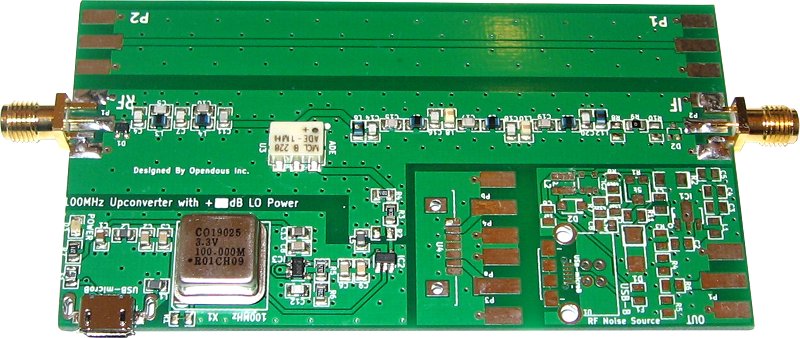
The Upconverter project went through a couple prototype phases:
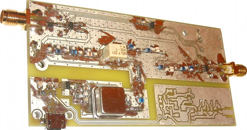
The second prototype more closely resembles the production boards:
There was also an attempt to design an Upconverter using only DigiKey sourceable parts but the conversion losses were on the order of 20dB.
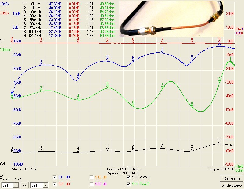
The standard 2-layer FR4 1oz. copper PCB from MyROPCB was tested with different SMA connectors as well as the production board and a SMA Cable of similar length. All of these are plots of uncompensated raw data.
The following data plot is of the PCB and CONSMA003.062 SMA connectors:
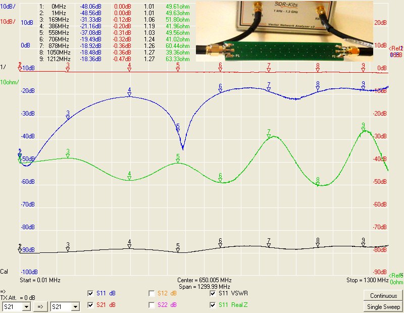
The following data plot is of the PCB and the production SMA connectors:

The following data plot is of a RG-316 coaxial SMA extension cable of similar length.
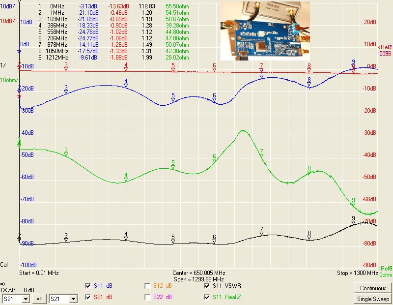
The following data plot is of the Upconverter in Passthrough mode:
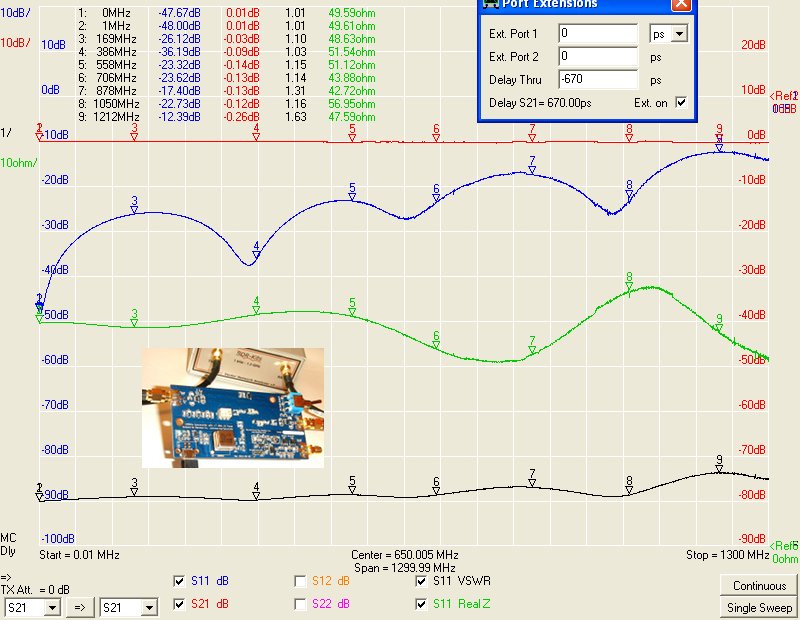
The following plot uses the same data as above but has been corrected for the length delay of the PCB trace. Using 165ps/inch=6.5ps/mm as the signal propagation time through copper on FR4 and a 103mm value for trace+connector length.
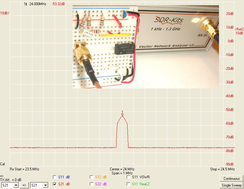
The following is the spectrum of a 24MHz oscillator (attenuated and DC-blocked). Note that the VNWA is not designed as a Spectrum Analyzer so the signal levels are not absolutely accurate but relative levels are useful.
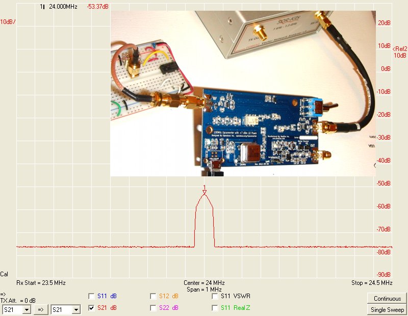
The following is the spectrum of the 24MHz oscillator in Passthrough Mode on the Upconverter:
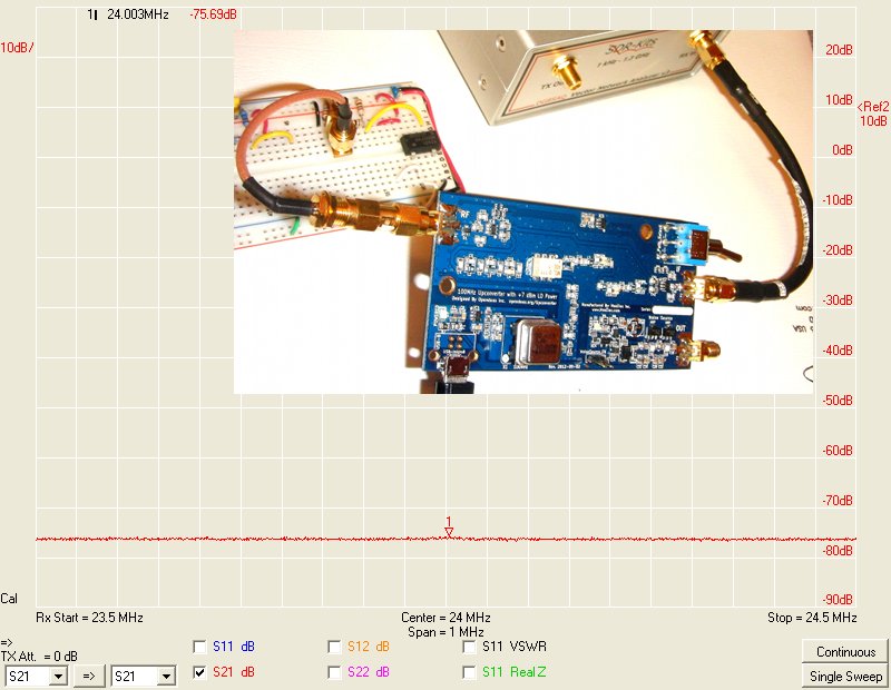
The following is the spectrum of the 24MHz oscillator in Upconvert Mode on the Upconverter. The filters are doing their job and removing the input signal.
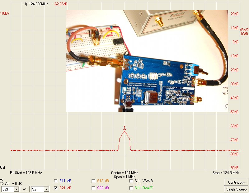
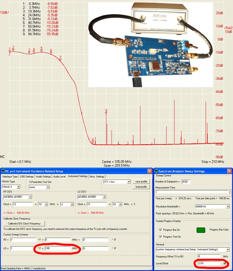
The following is the spectrum of the 24MHz oscillator upconverted to 124MHz. There is a ~9.35dB upconversion loss.
The following is the spectrum of the Upconverter with the tracking generator offset by 100MHz. This is a plot of the Upconversion losses which are below 10dB up to about 40Mhz, about 15dB at 50MHz, and hit the VNWA3 limits beyond 81MHz. The various peaks beyond are noise. The spectrum is vertically offset -2.61dB to make sure the 24MHz signal falls at 9.35dB loss, same as per the above Upconversion result for a 24MHz clock.

The following data plot is of the response of the first prototype Lowpass filter which was a 5th order filter.

The following data plot is of the response of the second prototype Lowpass filter which is a 7th order filter for a sharper transition band.

The following data plot is of the response of the first prototype Bandpass filter which is a 7th order filter.

The following data plot is of the response of the second prototype Bandpass filter which is the same 7th order filter as in the first prototype but with a different layout.

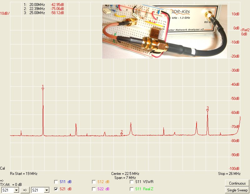
The following is the 19MHz to 26MHz spectrum of the 100MHz oscillator. There is a lot of noise mostly due to the breadboard construction of the test circuit but 20MHz clearly sticks out. All of these spectrum plots were taken using the longest possible VNWA3 sweep time. The VNWA3 is not designed as a spectrum analyzer so the exact values are not precise but the relative peak values are useful.
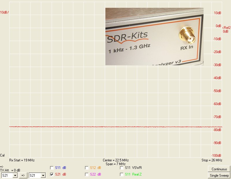
For comparison here is the 19MHz to 26MHz VNWA3 spectrum with open RX:
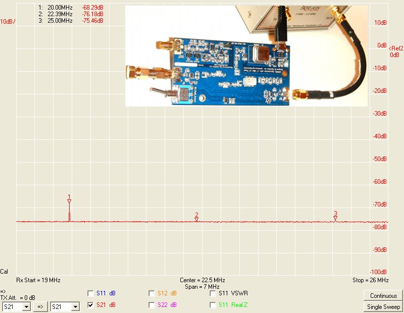
The following is the 19MHz to 26MHz spectrum at the IF port of the Upconverter with RF shorted with a 50-Ohm load and LO enabled (i.e., in Upconvert mode). The 20MHz internal LO frequency bleeds through but is significantly attenuated.

The following is the 19MHz to 26MHz spectrum at the RF port of the Upconverter with IF shorted with a 50-Ohm load and LO enabled (i.e., in Upconvert mode). The 20MHz internal LO frequency bleeds through but is significantly attenuated.
To reduce the internal LO frequency at the output and also help reduce LO harmonics, a Bessel band-pass filter was chosen for its minimal phase distortion to keep the LO signal as clean as possible.

The following is a data plot of the response of the originally designed LO Filter and attenuator.

The following is a data plot of the response of an updated LO Filter and attenuator.

Lowering the Q value of the L13 inductor increases losses by 4dB. Since it shorts to ground, the 3.76x greater resistance of the lower Q inductor leads to the greater power dissipation.
100MHz = 628318530 rad/s
Rl = wL / Q
AIMC-0805-6N8J-T : Rl = (628318530 * 6.8e-9) / 15 = 0.267
AISC-0805-R0068J-T : Rl = (628318530 * 6.8e-9) / 50 = 0.085
PM0805-6N8M-RC : Rl = (628318530 * 6.8e-9) / 60 = 0.071
From the above, it is clear that if you want to boost your LO level by about 4dB, replace L13 with lower Q inductors such as PM0805-6N8M-RC or AISC-0805-R0068J-T.
The following is a data plot of the response of the production LO filter with a PM0805-6N8M-RC inductor reworked into L13.

Although not recommended since the ADE-1 is only characterized for LO levels between +4dBm and +10dBm, you can gain another ~4dB by replacing L1 (47nH) with either a AISC-0805-R047G-T or PM0805-47NM-RC. An additional 0.5dB can be gained by removing R2, the 432 Ohm resistor closest to the LO buffer that makes up half the Pi Attenuator. However, it is not recommended to remove the full attenuator since it and the filter help convert the output impedance of the CMOS buffer into the 50 Ohm needed by the mixer.
The following data plot for the response of the production filter with no L13 shows you should not just remove it.

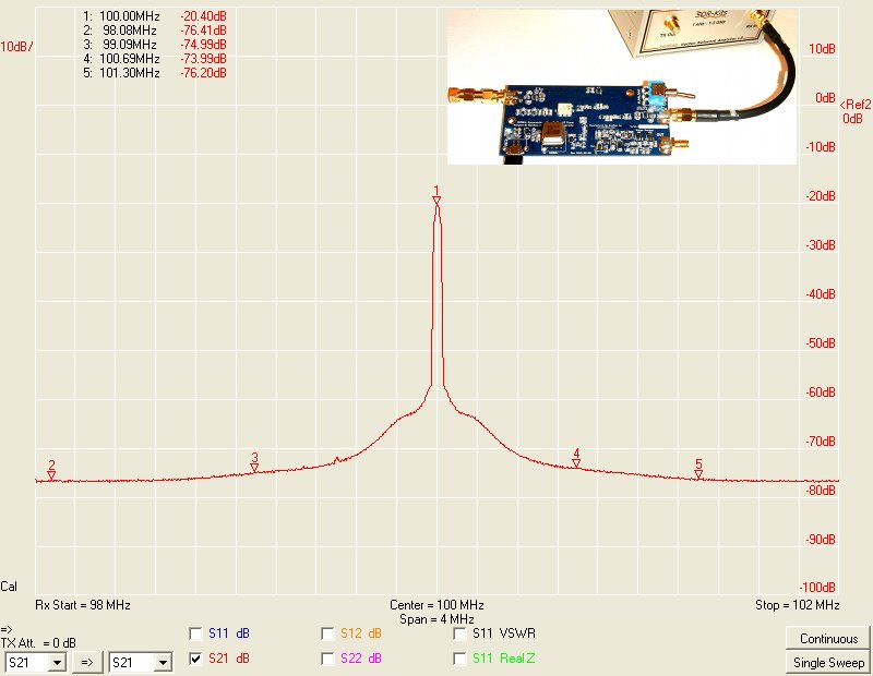
The following is the 98MHz to 102MHz spectrum at the IF port of the Upconverter with RF shorted with a 50-Ohm load and LO enabled (Upconvert mode). The VNWA3 is not designed as a spectrum analyzer so the exact values are not meaningful but the relative peak values are useful.
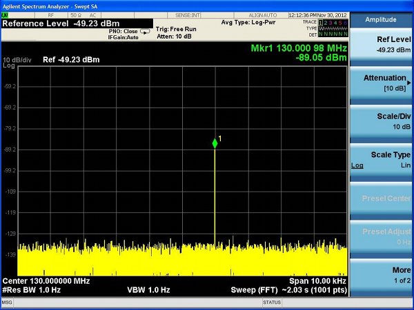
Here is sweep courtesy tikiarya of Avionics-Bangalore with a spectrum analyzer. The -48dBm makes more sense since the ADE-1 mixer has 43dB LO-to-IF isolation.

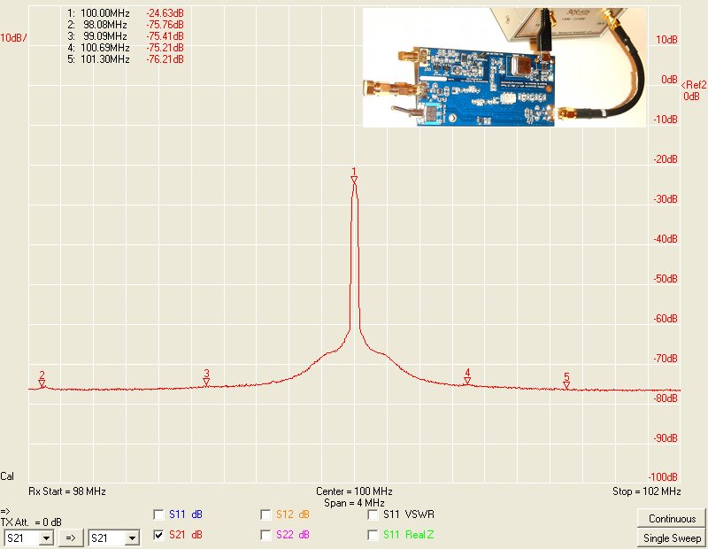
The following is the 98MHz to 102MHz spectrum at the RF port of the Upconverter with IF shorted with a 50-Ohm load and LO enabled (Upconvert mode).
The LO undergoes minimal shifting well within its 25ppm stability (100000000Hz(25/1000000)ppm=2.5kHz). Spectrum Analyzer results tikiarya of Avionics-Bangalore. Initial LO:
After warmup the Upconversion results shift <1kHz:
